100Gb/s Programmable Classifier Packet Switch: The synthesizable VHDL Programmable Classifier + 32x port packet switch IP core is able to link data ports [e.g. 1/10/25/100G SERDES PHY PCS MAC] and AXI4x128-bit Control Plane CPU ports. Allows classification via a synthesizable TCAM bank [up to 2048x] with CAM output processing to select insertion or extraction of Layer-2:3:4 headers including VLAN & MPLS.
Configurable for low power favoring large packets [27Mpp/s] or small packets at high rate [up to 400Mpp/s] this programable switch is available for FPGA or ASIC implementations. No special TCAM cells required - design is portable to any technology.
Encryption & Decryption IP Cores
AES High Speed [50/100/400Gb/s] Fixed Algorithm IP Core: The AES High Speed Fixed Algorithm Core is a VHDL implementation of the FIPS 197 AES Algorithm supporting only 256-bit key lengths. It supports the GCM mode per NIST SP-800-38D with AAD per ESPv3 IPSEC IPv4 & IPv4 specifications. Data Rate is dependent on implementation clock speed - Typical target implementation frequency is 400Mhz in high end Ultrascale+ of newer devices. At these clock rates the core is capable of 50Gb/s operation by default– and can be configured for 100-400Gb/s operation upon request. The core is available in non-redundant, lock step fail-safe or Macro-TMR configurations for operation in radiation environments.
AES Programmable Crypto IP Core: The AES Programmable Crypto IP Core is a VHDL implementation of the FIPS 197 AES Algorithm supporting only 128 & 256-bit key lengths. It supports ECB (forward and inverse cipher), GCM, OFB, CFB, CBC, CM (Counter) modes for Encrypt and Decrypt. The GCM mode is compliant with NIST SP-800-38D with support for variable length Additional Authentication Data (AAD) of 0-256-bits (compliant with MACSec, DTLS, IPSEC, and other specifications). The IV Generation is programmable to support No GHASH, GHASH of variable length (0-256-bit) IV inputs, or GHASH with xor with precomputed values (e.g. salt). Data Rate is dependent on implementation clock speed and the size of the data blocks fed to the core. Typical target implementation frequency is 125Mhz in mainstream Xilinx devices, and up to 250Mhz in high end Ultrascale+ of newer devices. At these clock rates the core is capable of 1Gb/s to 2Gb/s operation typically.
AES-256 Coprocessor IP Core: The AES-256-CoProcessor IP Core is a VHDL implementation of the FIPS 197 AES Algorithm supporting only 256-bit key lengths. It supports ECB (forward and inverse cipher), GCM (Encrypt & Decrypt), and CFB (Decrypt only) modes. The GCM mode is compliant with NIST SP-800-38D with support for variable length Additional Authentication Data (AAD) of 0-256-bits (compliant with MACSec, DTLS, IPSEC, and other specifications). Data Rate is dependent on implementation clock speed and the size of the data blocks fed to the core. Typical target implementation frequency is 100Mhz in mainstream Xilinx devices, and up to 250Mhz in high end Ultrascale+ of newer devices. At these clock rates the core is capable of 400Mb/s to 1.6Gb/s operation typically. To provide maximum flexibility the Y0 computation is done external to the core to support future standards and variable length IV inputs or salting. Contact SHA Solutions for details on how to compute the Y0 vector for various standards if required.
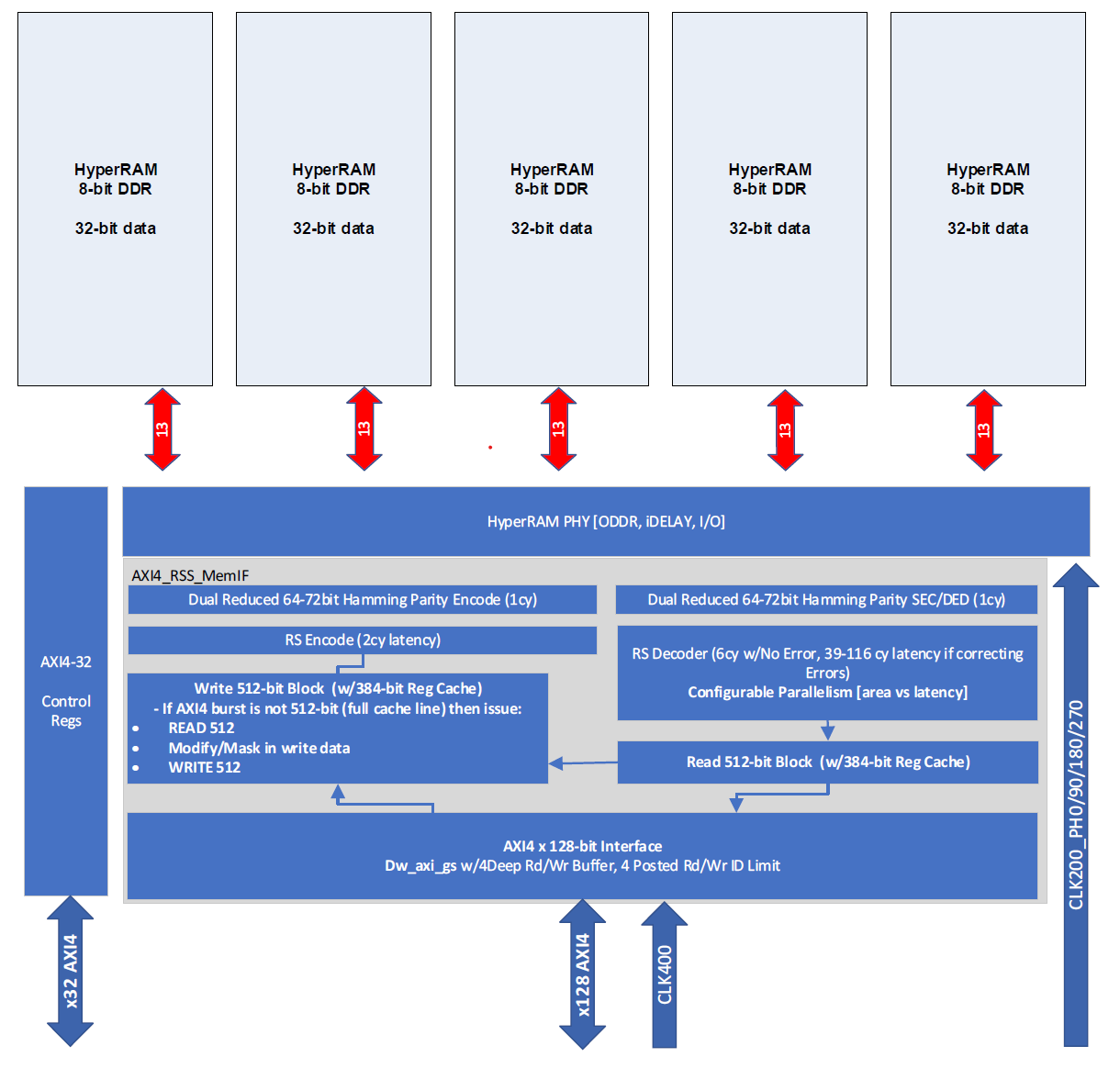
RT HyperRAM Memory Controller IP Core: The Radiation Tolerant (RT) HyperRAM IP Core is a VHDL & Verilog implementation that provides a AXI4-128 Slave to 5x External 8-bit DDR400 HyperRAM memories. It provides inline complex interleaved Error Correction capable of correcting 4Bytes (or 4 random bits) per 64Byte Block along with 2-bit random correction per 16Byte subblock within the 64B cacheline. The design is optimized for 64B cacheline accesses consistent with most ARM and RISC-V Embedded CPU designs. Read Modify Write for non-aligned or partial cacheline access is supported and handled internally by the core.
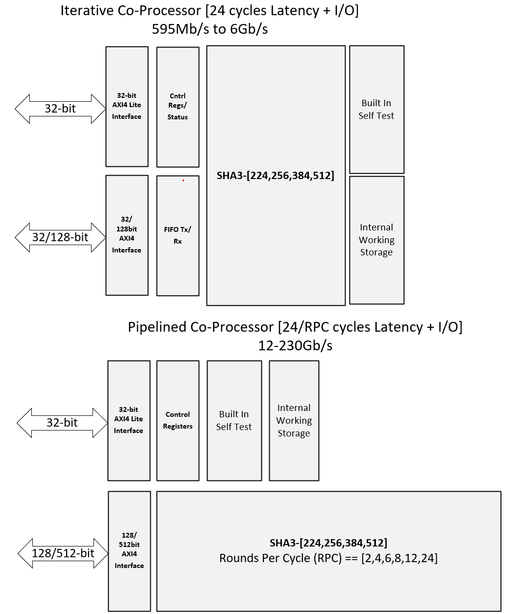
SHA3-[224,256,384,512] FIPS 202 CoProcessor IP Core: The SHA3 CoProcessor is available in a iterative version capable of 500Mb/s to 2.4Gb/s typical performance, or as a fully pipelined version capable of 115-230Gb/s in a Ultrascale+ FPGA. In a modern (22nm or below ASIC) technology the core achieves over 1Tb/s per instance. Design is fully synthesizable and portable with a built in self-test function. The IP is also available with Error Correction Coding (ECC) on all memories and storage, as well asoptionally with a High Assurance Fail Safe or Triple Modular Redundant (TMR) versions for use in systems where computations must be safe [e.g. IEC 61508,ISO 26262, DO-254 etc]. These techniques also make the core suitable for use in Radiation Environments [LEO, GEO orbits etc]
Building block IP Cores We develop and maintain a library of synthesizable technology agnostic IP cores that are licensable for FPGA or ASIC use. The benefits of our IP is that your not locked into any specific vendors technology and source code RTL is available for ease of use and customization.
Available building block IP: - 1/2.5/10/25G MAC & PCS - True Random Number Generators [TRNG] - Secure Hash (SHA)-256/384/512 per FIPS 180-2 - AESKey Wrap/Unwrap - AESKey Update